chemical etching process for sem .
chemical etching process for sem ; CS Cone ... with the Scanning Electron Microscope SummaryDifferent aspects of the chemical etching process for natural ...

 WhatsApp)
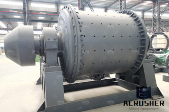
chemical etching process for sem ; CS Cone ... with the Scanning Electron Microscope SummaryDifferent aspects of the chemical etching process for natural ...
This sequence of patterning and etching is repeated multiple times during the chip making process. Etch processes ... physical and chemical etching such ...
Wet Chemical Etching Process of BST Thin Films for Pyroelectric Infrared Detectors Tianjin Zhang a, ... 2O = 1:25:50:20 was developed for BST films etching. SEM graph
To analyze the chemical etching process of InAs/GaSb ... SEM image of a cleaved mesa of the diode etched with the H 3PO 4/H 2O 2/H 2O solution at RT is shown in ...
A 3D Simulator for Silicon Anisotropic Wet Chemical Etching Process ... anisotropic etching process simulation ... chemical etching of crystalline ...
Chemical Etching (aka Photochemical Machining, ... Close up SEM image of partial ... For suspensions our photochemical etching process is capable of producing 1 mil ...
How to Acid Etch Steel. ... sulfate from coating the steel with a deposit of copper that will stop the etching process. ... The etching chemical, ...
chemical etching process. The chemical etchant used to ... Crosssectional SEM image of LEO GaN epilayer before etching process. (b–f) ...
Chemical etching technique for porous and finegrain YBa2Cu307x superconductors with or without silver ... and finegrain YBa2Cu307x superconductors with or ...
... assisted chemical etching process in ... chemical etching process on lithographically ... lithographically defined areas formation kinetics ...
... dissolution of agarose stamp into hot water demonstrates an environmentally friendly method by the moldassisted chemical etching process ... SEM images of ...
Scanning Electron Microscopy (SEM) ... Cleaning problems and chemical etching ; ... Hazard investigation of exfoliants from manufacturing process;
complementary chemical etching process, ... SEM images of an electrical discharge machined titanium microelectrode array that has undergone the chemical etching ...
This etching is a wetbased process that increases the ... (SEM) images of Si ... Nonlinear Etch Rate of AuAssisted Chemical Etching of Silicon ...
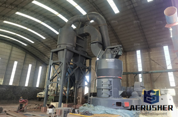
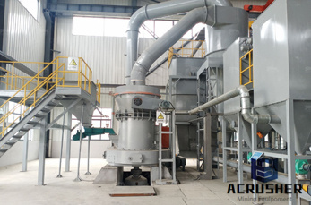
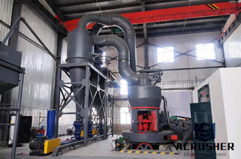
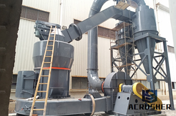
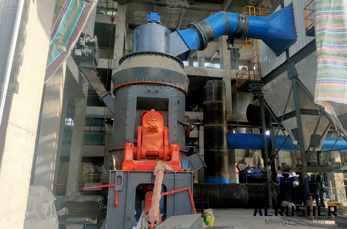
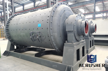
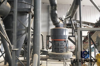
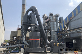
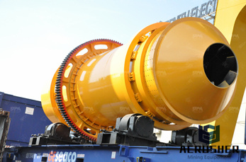
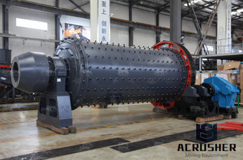
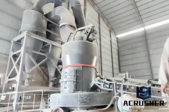
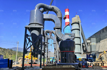
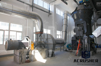
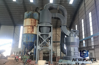
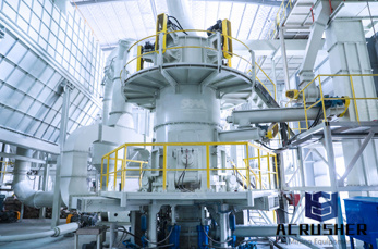
Home > Mining News > chemical etching process for sem. Information. Crushing Equipment; Grinding Equipment; Feeding Conveying; Screening Washing; Mobile .
In this paper, the dislocation in 50mm cz sapphire crystal had been observed by chemical etching with metallograph and sem ... it is challenging for the chemical etching ...
Alkali Anisotropic Chemical Etching of P ... SEM and FTIR spectroscopy. The ... The process of wet alkali anisotropic chemical etching process was monitored as the ...
Metalassisted chemical etching of CIGS thin films for grain ... wet chemical etching process to define CIGS ... can make the etching difference observable under SEM.
Inverse MetalAssisted Chemical Etching Produces ... 20 nm and AR > 35 using inverse metalassisted chemical etching ... and to optimize the etching process, we
WetChemical Etching and Cleaning of Silicon ... following is a typical RCA process; ... with all wetchemical etching solutions, ...
Electronassisted chemical etching of ... alterations that occur during electronassisted chemical etching of ... chemical etching process, ...
The Preparation of Silicon Nanowires Using MetalAssisted ... Silicon Nanowires Using MetalAssisted Chemical ... Chemical Etching, Silicon Nanowires, SEM.
Wet etching is a chemical etching process using a fluidic etchant. The advantage of the wet etching process for you as our customer is ... SEM cross section of an ...
To solve the problems generally encountered during the plasma electrolytic oxidation (PEO) of Al alloys with high Si content, a pretreatment of chemical etching was ...
WhatsApp)